作为一名电源研发工程师,自然经常与各种芯片打交道,可能有的工程师对芯片的内部并不是很了解,不少同学在应用新的芯片时直接翻到Datasheet的应用页面,按照推荐设计搭建外围完事。如此一来即使应用没有问题,却也忽略了更多的技术细节,对于自身的技术成长并没有积累到更好的经验。今天以一颗DC/DC降压电源芯片LM2675为例,尽量详细讲解下一颗芯片的内部设计原理和结构。
As a power supply R & D engineer, naturally often deal with various chips, some engineers may not understand the inside of the chip, many students directly turn to the application page of the new chip, according to the recommended design to build the periphery. In this way, even if the application is not a problem, it also ignores more technical details, and does not accumulate better experience for its own technical growth. Today, take a DC/DC step-down power chip LM2675 as an example, try to explain the internal design principle and structure of the next chip in detail.

LM2675-5.0的典型应用电路
Typical application circuit of LM2675-5.0
打开LM2675的DataSheet,首先看看框图
Open the LM2675 DataSheet and first look at the block diagram
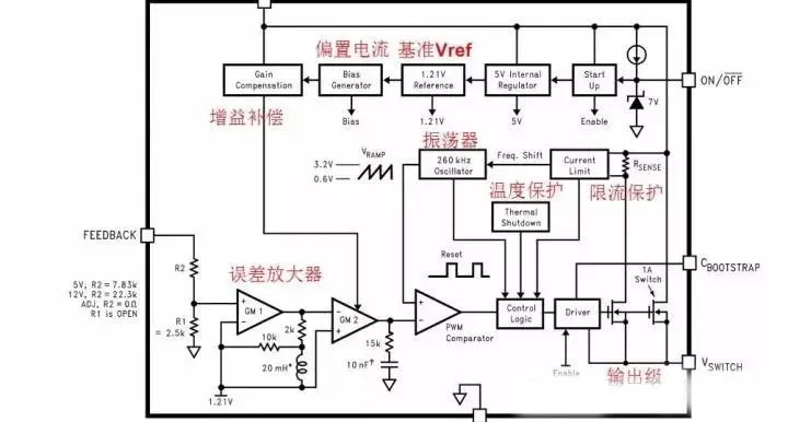
电源芯片的内部全部单元模块
All internal unit modules of the power chip
这个图包含了电源芯片的内部全部单元模块,BUCK结构我们已经很理解了,这个芯片的主要功能是实现对MOS管的驱动,并通过FB脚检测输出状态来形成环路控制PWM驱动功率MOS管,实现稳压或者恒流输出。这是一个非同步模式电源,即续流器件为外部二极管,而不是内部MOS管。
This diagram includes all the internal unit modules of the power chip. We have a good understanding of the BUCK structure. The main function of this chip is to drive the MOS tube and form a loop to control the PWM drive power MOS tube by detecting the output state through FB pin, so as to achieve stable voltage or constant current output. This is a non-synchronous mode power supply, that is, the continuous current device is an external diode, rather than an internal MOS tube.
下面咱们一起来分析各个功能是怎么实现的
Let's analyze how each function is implemented
01
基准电压
Reference voltage
类似于板级电路设计的基准电源,芯片内部基准电压为芯片其他电路提供稳定的参考电压。这个基准电压要求高精度、稳定性好、温漂小。芯片内部的参考电压又被称为带隙基准电压,因为这个电压值和硅的带隙电压相近,因此被称为带隙基准。
Similar to the reference power supply for board level circuit design, the internal reference voltage of the chip provides a stable reference voltage for the other circuits of the chip. This reference voltage requires high precision, good stability and low temperature drift. The reference voltage inside the chip is also called the band gap reference voltage, because this voltage value is similar to the silicon band gap voltage, so it is called the band gap reference.
这个值为1.2V左右,如下图的一种结构:
This value is about 1.2V, which is a structure of the following figure:
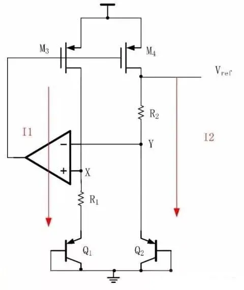
基准电压结构
Voltage reference structure
关键点:I1是正温度系数的,而Vbe是负温度系数的,再通过N值调节一下,可是实现很好的温度补偿!得到稳定的基准电压。
Key point: I1 is a positive temperature coefficient, and Vbe is a negative temperature coefficient, and then adjusted by the N value, but to achieve good temperature compensation! A stable reference voltage is obtained.
N一般业界按照8设计,要想实现零温度系数,根据公式推算出Vref=Vbe2+17.2*VT,所以大概在1.2V左右的,目前在低压领域可以实现小于1V的基准,而且除了温度系数还有电源纹波抑制PSRR等问题,限于水平没法深入了。
N The general industry according to 8 design, in order to achieve zero temperature coefficient, according to the formula calculated Vref=Vbe2+17.2*VT, so about 1.2V, currently in the low-voltage field can achieve less than 1V benchmark, and in addition to the temperature coefficient and power ripple suppression PSRR and other problems, limited to the level can not be further.
最后的简图就是这样,运放的设计当然也非常讲究:
The final schematic is like this, and the design of the op amp is of course very particular:

电路设计简图
Schematic diagram of circuit design
如图温度特性仿真:
Temperature characteristics simulation as shown in the figure:

温度特性仿真
Temperature characteristic simulation
02
震荡器OSC和PWM
OSC and PWM
我们知道开关电源的基本原理是利用PWM方波来驱动功率MOS管,那么自然需要产生振荡的模块,原理很简单,就是利用电容的充放电形成锯齿波和比较器来生成占空比可调的方波。
We know that the basic principle of the switching power supply is to use PWM square wave to drive the power MOS tube, then naturally need to generate the module of oscillation, the principle is very simple, is to use the charge and discharge of the capacitor to form a sawtooth wave and comparator to generate a square wave with adjustable duty cycle.
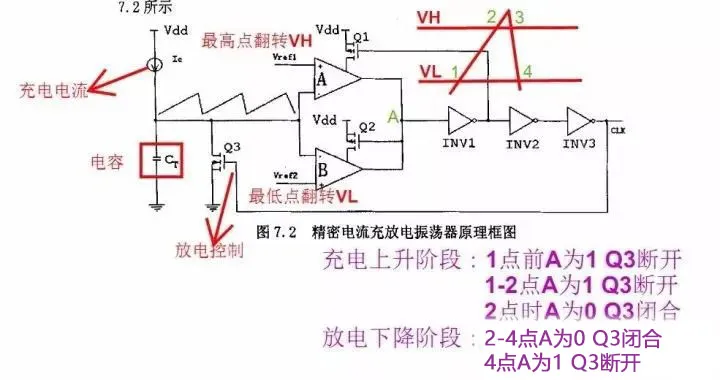
精密电流充放电振荡器电路图
Precision current charge-discharge oscillator circuit diagram
最后详细的电路设计图是这样的:
The final detailed circuit design is as follows:

LM2675-5.0的典型应用电路
Typical application circuit of LM2675-5.0
这里有个技术难点是在电流模式下的斜坡补偿,针对的是占空比大于50%时为了稳定斜坡,额外增加了补偿斜坡,我也是粗浅了解,有兴趣同学可详细学习。
A technical difficulty here is slope compensation in current mode, which is aimed at stabilizing the slope when the duty cycle is greater than 50%, additional compensation slope is added. I have a superficial understanding of it, and interested students can learn it in detail.
03
误差放大器
Error amplifier
误差放大器的作用是为了保证输出恒流或者恒压,对反馈电压进行采样处理。从而来调节驱动MOS管的PWM,如简图:
The function of the error amplifier is to ensure that the output is constant current or constant voltage, and to sample the feedback voltage. So as to adjust the PWM driving the MOS tube, as shown in the diagram:
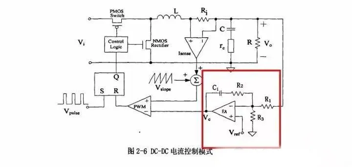
电流控制模式
Current control mode
04
驱动电路
Driving circuit
最后的驱动部分结构很简单,就是很大面积的MOS管,电流能力强。
The structure of the final driving part is very simple, which is a large area of MOS tube, and the current capacity is strong.
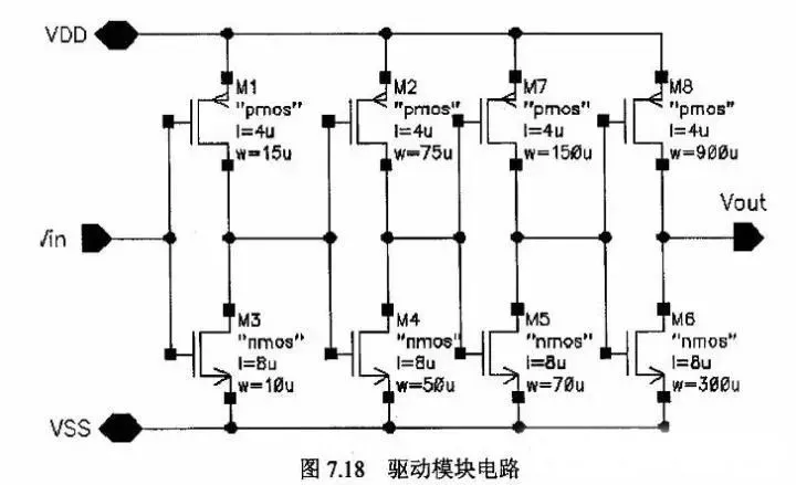
驱动模块电路图
Drive module circuit diagram
05
其它模块电路
Other module circuit
这里的其他模块电路是为了保证芯片能够正常和可靠的工作,虽然不是原理的核心,却实实在在的在芯片的设计中占据重要位置。
The other module circuits here are to ensure that the chip can work normally and reliably, although not the core of the principle, but really occupy an important position in the design of the chip.
具体说来有几种功能:
Specifically, there are several functions:
1、启动模块
1. Start the module
启动模块的作用自然是来启动芯片工作的,因为上电瞬间有可能所有晶体管电流为0并维持不变,这样没法工作。启动电路的作用就是相当于“点个火”,然后再关闭。如图:上电瞬间,S3自然是打开的,然后S2打开可以打开M4 Q1等,就打开了M1 M2,右边恒流源电路正常工作,S1也打开了,就把S2给关闭了,完成启动。如果没有S1 S2 S3,瞬间所有晶体管电流为0。
The role of the startup module is naturally to start the work of the chip, because it is possible that the current of all transistors is 0 and remains unchanged at the moment of power-on, so it cannot work. The function of the starting circuit is the equivalent of "lighting a fire" and then shutting it down. As shown in Figure: At the moment of power-on, S3 is naturally turned on, then S2 can be turned on M4 Q1, etc., then M1 M2 is turned on, the constant current source circuit on the right side works normally, S1 is also turned on, and S2 is turned off to complete startup. If there is no S1, S2, and S3, all transistor currents are zero in an instant.

启动电路
Starting circuit
2、过压保护模块OVP
2. overvoltage protection module OVP
很好理解,输入电压太高时,通过开关管来关断输出,避免损坏,通过比较器可以设置一个保护点。
It is well understood that when the input voltage is too high, the output is turned off by the switching tube to avoid damage, and a protection point can be set by the comparator.

过压保护电路
Overvoltage protection circuit
3、过温保护模块OTP
3. Overtemperature protection module OTP
温度保护是为了防止芯片异常高温损坏,原理比较简单,利用晶体管的温度特性然后通过比较器设置保护点来关断输出。
Temperature protection is to prevent abnormal high temperature damage to the chip, the principle is relatively simple, using the temperature characteristics of the transistor and then through the comparator set protection points to turn off the output.
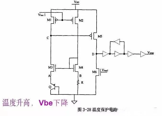
温度保护电路
Temperature protection circuit
4、过流保护模块OCP
4.overcurrent protection module OCP
在譬如输出短路的情况下,通过检测输出电流来反馈控制输出管的状态,可以关断或者限流。如图的电流采样,利用晶体管的电流和面积成正比来采样,一般采样管Q2的面积会是输出管面积的千分之一,然后通过电压比较器来控制MOS管的驱动。
In the case of an output short circuit, for example, the output current is detected to feedback the state of the output tube, which can be turned off or limited. In the current sampling shown in the figure, the current of the transistor is directly proportional to the area of the sampling tube. Generally, the area of the sampling tube Q2 will be one-thousandth of the output tube area, and then the drive of the MOS tube is controlled by the voltage comparator.

过流保护模块OCP
Overcurrent protection module OCP
还有一些其他辅助模块设计。
There are also some other auxiliary module designs.
06
恒流源和电流镜
Current mirror
在IC内部,如何来设置每一个晶体管的工作状态,就是通过偏置电流,恒流源电路可以说是所有电路的基石,带隙基准也是因此产生的,然后通过电流镜来为每一个功能模块提供电流,电流镜就是通过晶体管的面积来设置需要的电流大小,类似镜像。
Inside the IC, how to set the working state of each transistor, that is, through the bias current, the constant current source circuit can be said to be the cornerstone of all circuits, the band gap reference is therefore generated, and then through the current mirror to provide current for each functional module, the current mirror is through the area of the transistor to set the required current size, similar to mirroring.

曲率补偿的能隙基准
Energy gap reference for curvature compensation
nodule
小 结
以上大概就是一颗DC/DC电源芯片LM2675的内部全部结构,也算是把以前的皮毛知识复习了一下。当然,这只是原理上的基本架构,具体设计时还要考虑非常多的参数特性,需要作大量的分析和仿真,而且必须要对半导体工艺参数有很深的理解,因为制造工艺决定了晶体管的很多参数和性能,一不小心出来的芯片就有缺陷甚至根本没法应用。整个芯片设计也是一个比较复杂的系统工程,要求很好的理论知识和实践经验。最后,学而时习之,不亦说乎!
The above is probably the entire internal structure of a DC/DC power chip LM2675, which is also a review of the previous knowledge. Of course, this is only the basic architecture in principle, the specific design should also consider a lot of parameter characteristics, need to make a lot of analysis and simulation, and must have a deep understanding of the semiconductor process parameters, because the manufacturing process determines many parameters and performance of the transistor, accidentally out of the chip has defects or even can not be applied. The whole chip design is also a relatively complex system engineering, which requires good theoretical knowledge and practical experience. Finally, learn and learn, not also say!